INTRODUCTION
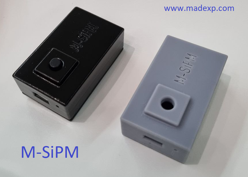
Yes, I did it! I finally designed and built a portable gamma-ray counter based on either a CdWO4 or CsI(Tl) scintillator, coupled with a 6×6 mm SiPM. Connected via Bluetooth to my smartphone, it will be very useful for detecting radioactive items at antique fairs and second-hand stores. Let’s go find some radium-painted clocks!
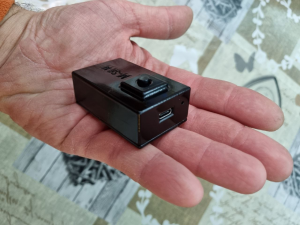
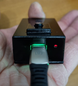
The crucial aspect was making it small enough to fit in a pocket, including a rechargeable LiPo battery and a USB-C connector for convenience. The scintillator crystal provides excellent sensitivity: initially, I prototyped the device with CsI(Tl), but to make it more compact, I chose CdWO4. Thanks to its higher density, CdWO4 can be as sensitive as CsI(Tl) while occupying a smaller volume.
Although this project is not open source, I am sharing the schematic and an example Android App created with App Inventor. You can download it here: p9A0i_bluetooth_dinamico.
COPYRIGHT NOTICE
You are welcome to build your own version of the circuit/software for personal use only, either by taking inspiration from my schematic or by copying it.
However, you may not create a commercial product without infringing on my copyright.
© Papadopol Lucian Ioan 2021. All rights reserved.
GENERAL SCHEMATIC
This is the general schematic, provided to give you an overview of the design. The following sections explain some key parts in more detail.
Essentially, the schematic consists of five functional blocks:
- MCU STM32L053: Counts pulses, controls power to peripherals, and sends data via UART.
- TIA + SiPM: Handles pulse extraction and shaping.
- SiPM Bias Supply: Provides the necessary bias voltage for the SiPM.
- LiPo Charger and Voltage Regulators: Manage battery charging and supply stable voltages.
- Bluetooth Module: Enables wireless communication.
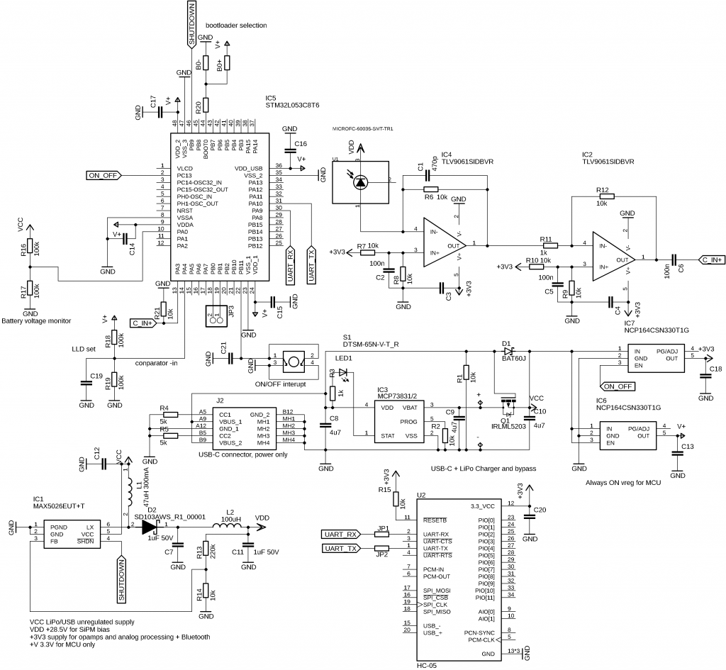
The LiPo charger and Bluetooth module are standard building blocks, requiring little explanation. For voltage regulators, one is always active to power the MCU, while the second is controlled by the MCU to enable or disable the Bluetooth, op-amp chain, and bias supply.
The push button in the middle of the schematic has a specific function: it triggers an Interrupt Service Routine (ISR) that instructs the MCU to either continue operating or enter standby mode.
How does the MCU detect and count pulses? It uses the internal OPAMP. The pulse input C_IN+ is connected to the +IN pin of the internal comparator. A voltage divider (R18/R19) sets the Lower Level Discriminator (LLD). In the schematic, it is shown as 1/2 VCC using a 100k/100k divider. This is only a placeholder: you must adjust the divider based on the noise level observed at the C_IN+ pin with an oscilloscope. I set mine to about 60 mV. When a pulse exceeds the LLD, the comparator triggers an ISR, which increments a counter. Once per second the counter is read, sent via UART, and then reset.
SiPM bias PSU
This schematic generates a +28.5 V bias from a single-cell LiPo (~4 V) with about 10 mV peak-to-peak noise. It is derived directly from the MAX5026 datasheet (please read it!).
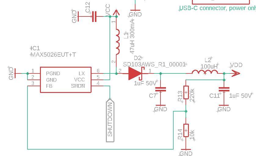
R13–R14 set the output voltage. L1 is a 47 µH inductor with 300 mA current capability (Würth brand). The output ripple filter is a CLC cell: C7–L2–C11. Use high-quality 1 µF / 50 V ceramic or tantalum capacitors.
TIA
This part of the schematic, despite its simplicity, took me the most time to optimize. The first op-amp works as a Transimpedance Amplifier (TIA). Its gain is set by the 10k feedback resistor. The 470–680 pF capacitor in parallel compensates for the SiPM capacitance. You must choose this capacitor carefully to prevent oscillations in the stage.
The second stage is an inverting amplifier with ~10× gain, adjustable as needed. Each op-amp is biased at 1/2 VCC using 10k/10k voltage dividers on the –IN pin. This arrangement allows negative pulses at the TIA output, which are then inverted by the second gain stage.
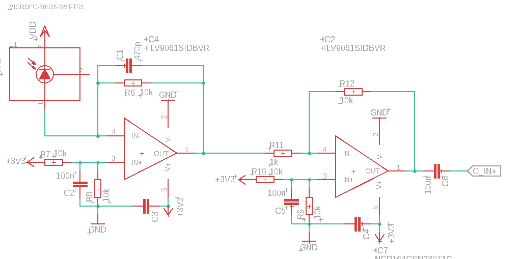
The op-amp must have at least 1 MHz GBP for CdWO4 and 10 MHz GBP for CsI(Tl).
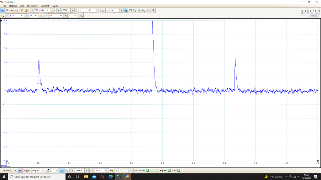
This is how the pulses appear at the output of this stage. The quality is sufficient for basic gamma spectroscopy. My plan is to extend the project with an ADC input bypass and configure the MCU’s ADC to run in continuous mode with DMA, implementing software-based peak detection. I will update this page as soon as possible.